Precision component manufacturing (e.g., aerospace parts, medical implants, electronic elements) demands extremely tight tolerances, material performance, and surface quality. Below are critical factors that must be strictly controlled during production.
Material Purity: High-precision parts often require high-purity metals (e.g., titanium alloys, stainless steel 316L) or specialty alloys (e.g., Invar, nickel-based superalloys).
Heat Treatment: Stress relief through annealing, quenching, or aging to prevent machining deformation (e.g., T6 heat treatment for aluminum).
Material Certification: Requires material test reports (MTRs) to ensure compliance with standards (e.g., ASTM, AMS).
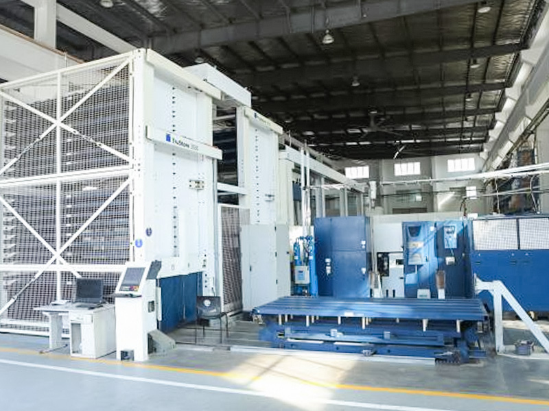
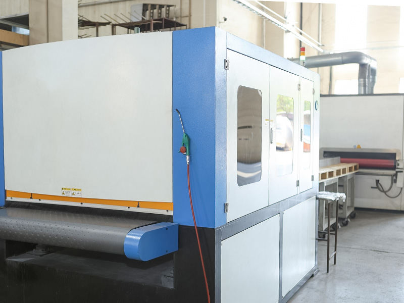
Ultra-Precision Cutting/Grinding:
Turning/milling tolerances within ±0.005mm (e.g., optical lens molds).
Grinding for hard materials (e.g., ceramics, tungsten carbide), achieving surface roughness Ra ≤0.1μm.
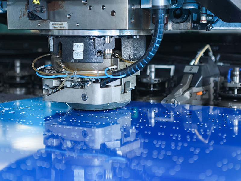
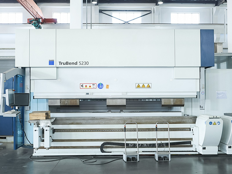
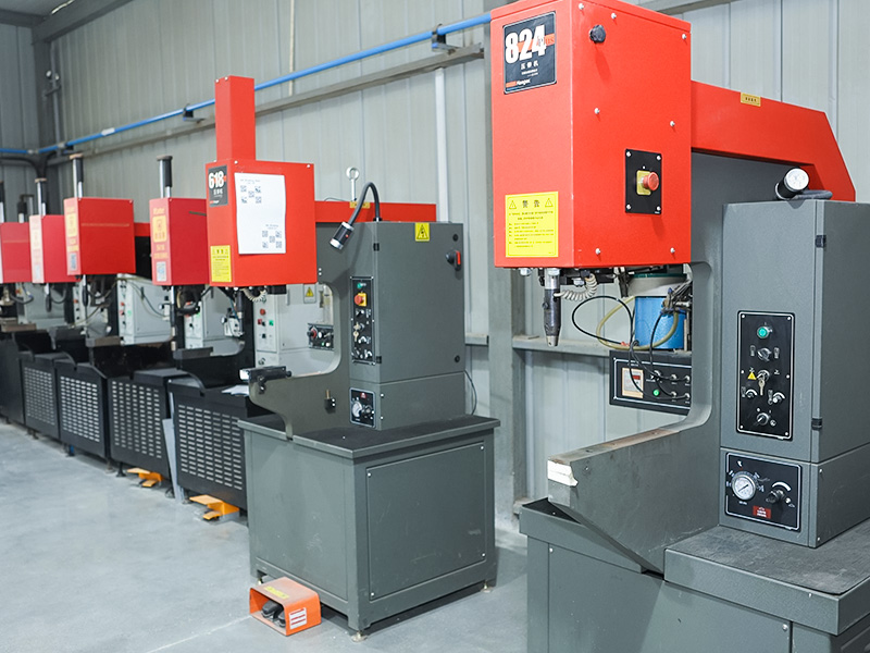
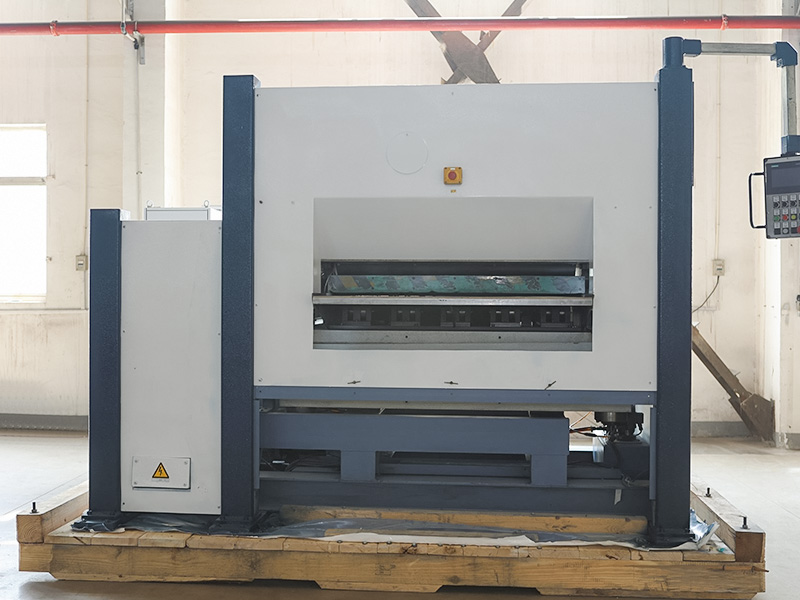
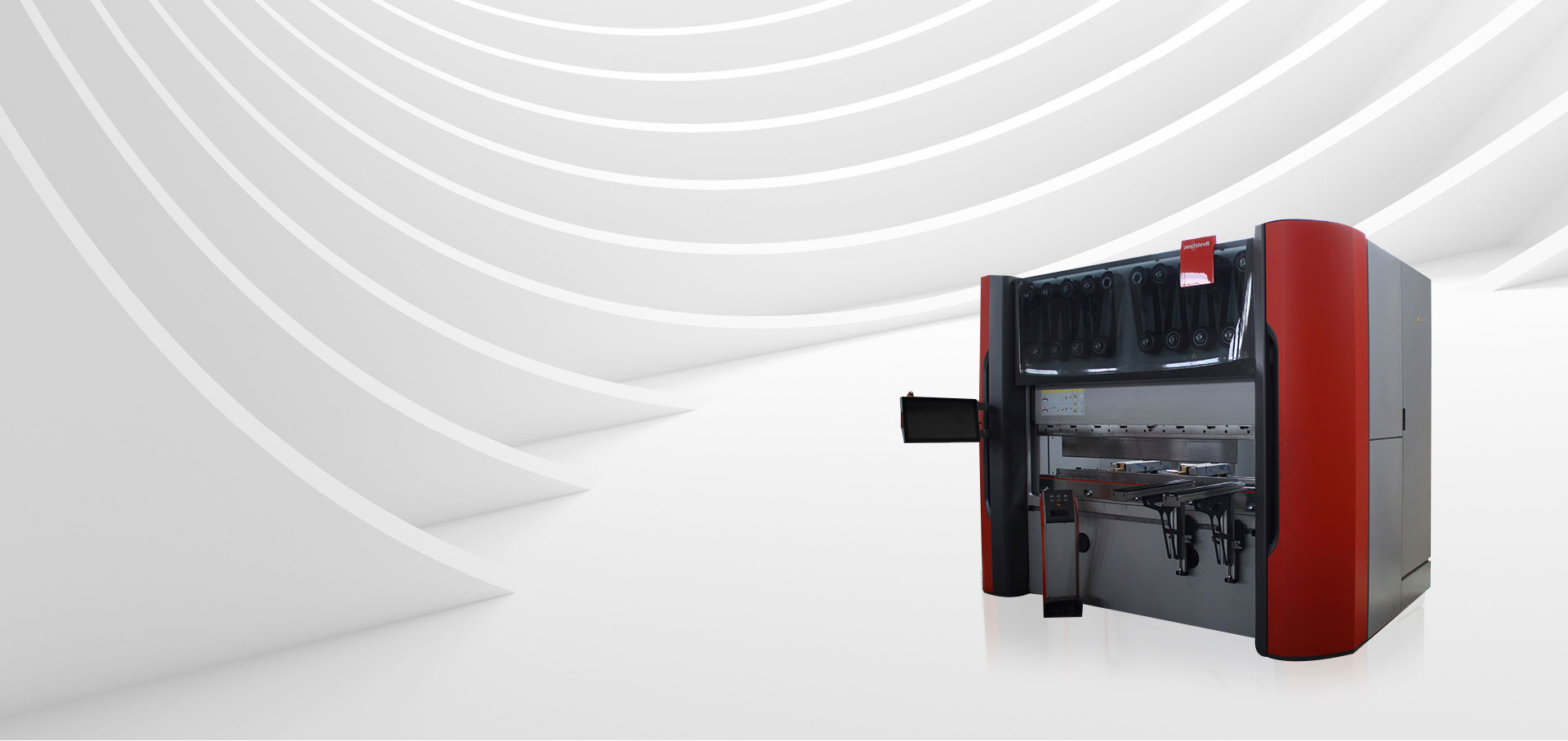
Micron-Level Stamping/Bending:
Bend angle control within ±0.1°, with real-time laser feedback.
Progressive die stamping for micro-components (e.g., SIM card trays).
Electrical Discharge Machining (EDM): For complex high-hardness shapes (e.g., turbine blade cooling holes).
Laser Processing: Cutting/welding ultra-thin materials (e.g., 0.05mm stainless steel tubes for heart stents).
Electrochemical Machining (ECM): Stress-free machining of conductive materials (e.g., jet engine blades).
Critical Dimensions: Clearly marked (e.g., bearing mating surfaces as key characteristics, tolerance ±0.002mm).
Geometric Tolerances:
Flatness/parallelism ≤0.01mm (e.g., semiconductor wafer carriers).
Concentricity ≤φ0.005mm (e.g., fiber optic connectors).
Measurement Tools:
Coordinate Measuring Machines (CMM) for full-dimension inspection (accuracy ±1μm).
Optical profilometers for micro-surface defects (e.g., scratch depth ≤0.2μm).
Surface Finish:
Hydraulic valve cores require Ra ≤0.4μm (mirror polishing/honing).
Medical implants need electropolishing to remove micro-cracks.
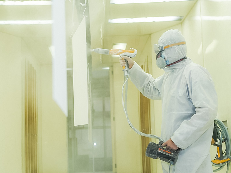
Corrosion Protection:
Hard anodizing for aluminum (20–50μm thickness).
PTFE or ceramic coatings for aerospace components.
Cleanliness Control:
Semiconductor parts require Class 100 cleanrooms.
Ultrasonic cleaning before assembly (particle residue ≤5μm).
Temperature/Humidity Control:
Climate-controlled workshops (20±1°C) to prevent thermal distortion (e.g., precision bearing machining).
Humidity ≤40% to avoid oxidation (e.g., magnesium alloy parts).
Equipment Calibration:
CNC machines calibrated every 8 hours via laser interferometry.
Press machines regularly verified for tonnage accuracy (±1%).
First Article Inspection (FAI): Full-dimension reports require customer approval.
Process Monitoring: SPC for critical parameters (e.g., CPK ≥1.67).
Traceability: Batch records of process parameters (e.g., laser power, cutting speed).
| Industry | Key Requirements |
|---|---|
| Aerospace | NADCAP certification, fatigue life testing (e.g., 10^7 cycles). |
| Medical Implants | Biocompatibility (ISO 13485), sterilization validation (EO/γ-ray). |
| Optical Components | Light transmittance ≥99.8%, surface defect standards (e.g., MIL-PRF-13830B). |
Smart Manufacturing: AI-driven real-time parameter adjustment (e.g., adaptive cutting force control).
Hybrid Additive/Subtractive: 3D printing near-net shaping + precision finishing.
Nanoscale Machining: Focused ion beam (FIB) for chip-scale structures.
Precision manufacturing hinges on end-to-end process control—any oversight (e.g., a 0.01mm error in a spacecraft bolt causing launch failure) can lead to catastrophic batch rejection.


 +86-13771171111 +86-13338110517

 English
 中文简体
中文简体 日本語
日本語 Deutsch
 Español
 Bahasa Melayu